研究室での研究活動 Research Activities in The Lab
人間の身体や、世界・自然・宇宙など、すべては量子でできています。量子とは物質やエネルギーの最小単位であり、原子は量子から構成され、電子もまた量子です。現在、人間が手にしているナノテクノロジーと呼ばれる技術では原子を1個単位で制御することができ、さらに、量子ナノエレクトロニクスの分野では電子を1個ずつ操作しています。しかし、原子や電子を自在に制御することはとても難しく、その理解には量子力学と呼ばれる新しい物理学が必要です。量子力学を基礎とするナノテクノロジーやナノエレクトロニクスの研究の進展により、近年、その実現が極めて困難とされてきた量子計算機が姿を現しはじめています。量子計算機は原理的に強大な演算能力を有していることから究極の計算機と考えられ、人間は、夢と思われてきた極限の性能を有する新型計算機を現実のものとしつつあります。 我々の研究室では、原子や電子を1個ずつ操作する究極的な研究を行っています。そのためには、量子力学の知識やナノテクノロジーやナノエレクトロニクスに関する様々な実験の技能・経験など、膨大な知見や技量を身に付ける必要があります。一方、近年、人工知能の性能も極めて大きく向上してきました。そこで我々は、量子の世界の難しい研究や実験を人間が行うのではなく、量子計算機をもとに適切に設計された量子人工知能マシンに実行させることを考えています。 将来、量子人工知能に支援された量子状態の制御技術が量子デバイスである量子ビットを自律的に作製し、量子計算機のような強力なコンピュータを生み出す。それがより高等な量子人工知能を表現し、より高度な量子計算機を生み出す。未来では、人間ではなくマシンが研究活動を行うかもしれませんね。知能情報システム工学科HPでの研究室紹介
The human body, the world, nature, the universe, everything is made of quantum. Quantum is the smallest unit of matter and energy, atoms are composed of quantum, and electrons are also quantum. Current nanotechnology controls atoms on a unit basis, and furthermore, in nanoelectronics, electrons are operated one by one. However, controlling atoms and electrons is very difficult, and a new physics called quantum mechanics is needed to understand it. These studies are making quantum computers a reality. In our laboratory, we are conducting ultimate research that manipulates atoms and electrons one by one. It requires a vast amount of knowledge and skills, such as knowledge of quantum mechanics and experimental skills and experience. On the other hand, the performance of artificial intelligence has greatly improved in recent years. So we are thinking of having the difficult research of the quantum world executed by appropriately designed artificial intelligence (machines) instead of humans. Quantum state control technology supported by artificial intelligence autonomously manufactures quantum devices and produces powerful computers like quantum computers. It expresses more advanced artificial intelligence and produces more advanced quantum computers. In the future, machines, not humans, may conduct research activities.
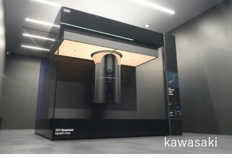
量子ゲート型量子計算機 Gate-Based Quantum Computers
D. Tsukayama, J. Shirakashi, T. Shibuya and H. Imai, AIP Advances 15 (2025) 015226.
D. Tsukayama, J. Shirakashi and H. Imai, Jpn. J. Appl. Phys. 62 (2023) 088003.
現在の量子計算機は、ノイズによる計算エラーが生じるものの、膨大な情報量を高速に処理できる計算能力を有する。このような量子計算機を利用する方法として、従来の計算機による計算の正確さを組み合わせた変分量子アルゴリズムが提案されている。このアルゴリズムでは、量子計算機から得られる結果がより質の高い解に近づくように、量子計算機のパラメータを従来の計算機で繰り返し調整することで問題の解を探索する。しかし、質の悪い解が数多く存在するために、従来の解探索手法では最適な解を発見できない場合がある。この課題に対処するため、物理的プロセスを模倣した最適化手法であるCoolMomentum法を導入した。CoolMomentum法は、解探索が進むにつれて探索範囲を徐々に狭めることで、質の悪い解を避けて最適解を発見する手法である。本手法は、量子計算機の計算能力を従来の計算機で実行可能なアプローチによって改善できることを示し、新薬の開発、物流や金融の最適化、AI・機械学習などの分野に貢献できる可能性を秘めている。
We compare the use of adaptive moment estimation (ADAM), simultaneous perturbation stochastic approximation (SPSA), Nakanishi-Fujii-Todo method (NFT), and CoolMomentum in a variational quantum eigensolver. Using a random weighted max-cut problem, we numerically analyze these methods and confirm that CoolMomentum performs better than the other methods. ADAM and SPSA tend to get trapped in local minima or exhibit infeasible optimization durations. Although NFT exhibits fast convergence, it tends to suffer from local minima similar to ADAM and SPSA. Contrarily, CoolMomentum shows a higher accuracy under noiseless and realistic hardware noise conditions.
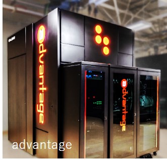
量子アニーリング型量子計算機 Quantum Annealers
Y. Yoneda, M. Shimada and J. Shirakashi, Appl. Phys. Express 16 (2023) 057001.
J. Artag, M. Shimada and J. Shirakashi, Conference Proceedings, 2023 IEEE International Conference on Quantum Computing and Engineering (QCE). 近年の社会システムの大規模・複雑化に伴い、その解析や最適化への必要性が高まっている。その課題の多くは組合せ最適化問題と呼ばれ、解空間が膨大にあるために従来のコンピューティングでは多大な時間を要する。そこで、新たな原理を用いた次世代のコンピュータに大きな期待が寄せられている。量子アニーリングマシンは組合せ最適化問題を解く計算機として知られ、2011年にD-Wave社が世界で初めて商用化し、大きな話題を呼んだ。この原理には磁性体の振る舞いを模擬した統計力学上のモデルであるイジングモデルが用いられており、超伝導磁束量子ビットによって物理実装されている。量子アニーリングマシンでは、組合せ最適化問題をイジングモデルにマッピングすることにより、量子重ね合わせを利用して自然収束動作による効率的な解探索を行うことができる。一方、これまで我々は、フィードバック制御型エレクトロマイグレーション(Feedback-Controlled Electromigration: FCE)法を金属細線に適用し、Au原子接合の作製および原子移動制御を行ってきた。より精緻に原子の移動制御を行うためには実験パラメータを最適化する必要があるが、FCE法には数多くの実験パラメータが存在し、人間が最適な実験パラメータを発見することは極めて困難である。そこで、我々は、FCE法の実験パラメータの最適化を組合せ最適化問題と捉え、量子アニーリングマシンを用いて自律的に決定する手法を検討した。 本研究では、FCE法のパラメータの一つである印加電圧のフィードバック量VFBのスケジュールに着目した。FCE実験により得られたデータからVFBの原子の移動制御性における評価を行い、その評価を最大化する実験スケジュールが最適解となるように定式化した。量子アニーリングマシンを用いて解探索を行い、SAやSQAのシミュレーションと比較し、本手法における量子アニーリングマシンの有用性や可能性を検討した。その結果、物理ハードウェアとしての量子アニーリングマシンはシミュレーションの演算精度に及ばなかったが、問題サイズを小さくすれば、シミュレーションと同等の最適な実験スケジュールを得ることができた。このスケジュールを用いたFCE実験でAu原子接合における量子化コンダクタンスの制御性の向上が示されており、このことから、量子アニーリングマシンがAu原子接合の量子化コンダクタンスを制御するFCEの実験パラメータを最適化できることが示唆された。Feedback-controlled electromigration (FCE) is employed to control metal nanowires with quantized conductance and create atomic junctions. The FCE scheme is commonly implemented using many experimental parameters, and determining the optimal FCE parameters can be regarded as a combinatorial optimization problem. The D-Wave quantum annealer has attracted attention for its hardware implementation of quantum annealing (QA), which is a heuristic algorithm for solving combinatorial optimization problems. This study developed a QA approach for optimizing the FCE parameters and executed it on a quantum annealer. The results and performance were compared with those of a classical solver.
量子インスパイアード型量子計算機(イジングマシン)Quantum-Inspired Ising Machines
A. Yoshida, T. Miki, M. Shimada, Y. Yoneda and J. Shirakashi, Appl. Phys. Express 15 (2022) 067002.
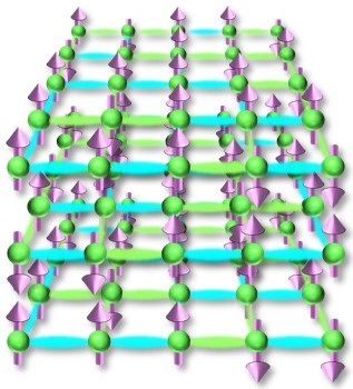
組合せ最適化問題は工学や金融、化学といった実社会上のあらゆる場面に存在し、ナチュラルコンピューティングの一種であるイジングスピンコンピューティングによる解決が行われてきた。特に、量子効果を用いて最適解を求めることが可能な量子アニーリングマシンは、量子の性質を活かした高速性により大きな注目を集めている。一方、これまでの古典的な論理ビットとは振る舞いが異なる量子ビットを用いているためハードウェアの制約も多く、性能向上に向けた技術の進展が図られている。これに対し、量子技術を半導体論理回路上で模倣した量子インスパイアードイジングマシンでは、既存の半導体集積回路技術を用いることで量子アニーリングマシンにおける制約を解決することができる。本研究では、量子インスパイアードイジングマシンによる大規模かつ複雑な組合せ最適化問題の求解を目指し、本技術に有効なスピン判定アルゴリズムである抽出型多数決論理(Extraction-Type Majority Voting Logic: E-MVL)を提案した。 これまで我々は、スピン間の交換相互作用がXNORゲートと等価であることを用いて、論理ゲートで表現されたイジングスピンコンピューティングについて検討してきた。この新しい計算機では、論理ゲートを用いて解探索を行うためのスピン判定論理が必要となり、大規模な組合せ最適化問題を高精度に解くことができる高性能なスピン判定論理が必要とされる。そこで我々は、スピン間結合のスパース化の導入により演算性能の向上を狙う、抽出型多数決論理(Extraction-Type Majority Voting Logic: E-MVL)を提案した。本研究ではE-MVLによるスピンダイナミクスをボルツマン分布に基づく理論的な振る舞いと比較することで、E-MVLの持つ物理的な特性について明らかにした。その結果、スピンに熱を与えた際の振る舞いをスパース化によって表現することができ、物理的なスピンにおける温度とE-MVLにおける制御パラメータであるSparsityが等価であることが明らかとなった。さらに、E-MVLの性能を大きく左右する演算パラメータの最適化を行うことで、高度に最適化された古典アルゴリズムに対して演算精度の向上や本質的な高速化が確認された。以上より、本研究で提案したE-MVLは、量子インスパイアードイジングマシンに有効であり、大規模な社会課題を解決できることが示唆された。We introduce extraction-type majority voting logic (E-MVL) that explores the ground state of an Ising spin model. The spin dynamics of E-MVL approximately follow that of thermal spins based on the Boltzmann distribution, even though E-MVL intentionally reduces the information of the problem graph by controlling the sparsity of problem graphs to realize high-speed calculation. We solved the Sherrington-Kirkpatrick spin-glass model using E-MVL and simulated annealing (SA). The probability of obtaining a solution with a 99% E-MVL accuracy is maintained at approximately 85% over the problem size, and E-MVL achieves a high accuracy compared to that of SA.
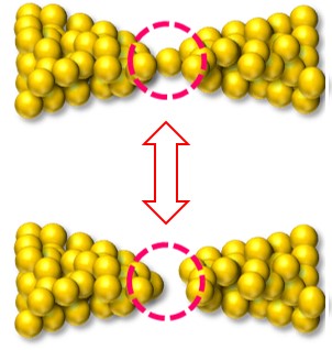
ナノギャップ/原子接合での原子操作 Atom Manipulation in Nanogaps/Atomic Junctions
S. Sakai, Y. Hirata, M. Ito and J. Shirakashi, Sci. Rep. 9 (2019) 16211.
S. Kayashima, K. Takahashi, M. Motoyama and J. Shirakashi, Jpn. J. Appl. Phys. 46 (2007) L907-L909.
社会システムが大規模化、複雑化するにつれ、その解析や最適化が重要な課題となっている。これらの課題の多くは、組合せ最適化問題と呼ばれる、従来のコンピューティング技術が苦手とする数学的問題に帰着する。近年、最適化問題をイジングスピンモデルの基底状態探索問題に変換することで、効率よくこの問題を解く試みが注目を集めている。イジングスピンモデルは、磁性体におけるスピンの性質を表す統計力学上のモデルであり、近年ではハードウェアへの実装が数多く報告され、イジングモデルの持つ能力をどのように活用するかの議論や検討が幅広く行われている。我々は、多くの制御パラメータの存在によりそれらの組合せで表現される、解空間が膨大となる現実の量子実験系に対し、本モデルを適用することを検討した。具体的には、金属細線におけるナノギャップや原子接合の作製手法として知られている、フィードバック制御型エレクトロマイグレーション(Feedback-Controlled Electromigration: FCE)法への適用を行い、量子化コンダクタンスを制御する実験パラメータの決定を行った。実際に、最適化された実験パラメータをFCE法に適用し、イジングモデルの有用性を検討した。 本実験では、Au原子接合における原子移動制御に必要な実験パラメータに対し、イジングモデルによる実験パラメータの探索と最適化を行った。はじめに、FCE法におけるパラメータ選択問題を組合せ最適化問題として数理定式化し、イジングスピンモデルの基底状態が実験パラメータの最適な適用スケジュールを表すようにハミルトニアンを設定した。その後、FCEの実験データより算出した評価指標をイジングスピンモデルへマッピングし、解探索を行った。その結果、イジングモデルを用いることで、最適な実験制御パラメータを自律的に決定可能であることが示された。さらに、最適化された実験パラメータスケジュールをAu原子接合作製実験へ適用した。その結果、パラメータをランダムに設定した場合と比べ、Au原子接合における原子操作の制御性が優れていることが確認された。これより、イジングモデルによる実験パラメータの探索と最適化によって、Au原子接合における原子の量子状態の自律的な制御が可能であることが示された。さらに、3種類のFCE実験パラメータである、電圧フィードバック量VFB、閾値コンダクタンスGTHおよび電圧増加幅VSTEPに対し、イジングモデルを用いた静的及び動的な実験パラメータの自動決定システムを構築した。静的な実験パラメータ決定手法では、FCE法におけるパラメータ選択問題を組合せ最適化問題としてイジングモデルへマッピングし、解探索を行った。これより、VFB、GTHおよび VSTEPのスケジュールを決定し実際にFCE法へ適用した結果、量子化コンダクタンスの制御性向上を確認した。また、動的な実験パラメータ決定手法では、FCEの進行状況に応じてVFB、GTHおよび VSTEPをリアルタイムに探索・決定しながら、FCEへ自動的に適用するイジングモデルを構築し、FPGAへシステム実装した。FPGAを用いた動的なシステムでは、実験を繰り返すことで交換相互作用をデータベースへ蓄積・更新し、原子の操作に対する評価指標の向上が明らかとなった。これらより、イジングモデルを用いた人の手を介さないFCE実験パラメータの決定手法により、Au原子接合を自律的・安定的に形成可能であることが示唆された。Feedback-controlled electromigration (FCE) is employed to control metal nanowires with quantized conductance and create nanogaps and atomic junctions. In the FCE method, the experimental parameters are commonly selected based on experience. However, optimization of the parameters by way of tuning is intractable because of the impossibility of attempting all different combinations systematically. Therefore, we propose the use of the Ising spin model to optimize the FCE parameters, because this approach can search for a global optimum in a multidimensional solution space within a short calculation time. The FCE parameters were determined by using the energy convergence properties of the Ising spin model. We tested these parameters in actual FCE experiments, and we demonstrated that the Ising spin model could improve the controllability of the quantized conductance in atomic junctions. This result implies that the proposed method is an effective tool for the optimization of the FCE process in which an intelligent machine can conduct the research instead of humans.
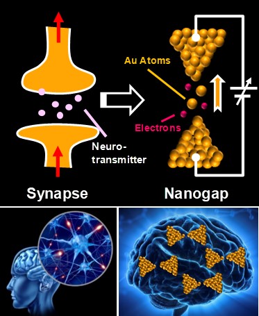
脳型コンピューティングアーキテクチャ:人工シナプス素子、リザバーコンピューティング Brain-Inspired Computing: Artificial Synapses, Reservoir Computing
K. Sakai, Y. Tanaka, M. Yagi, M. Ito and J. Shirakashi, ACS Appl. Electron. Mater. 7 (2025) 8400.
K. Sakai, M. Yagi, M. Ito and J. Shirakashi, J. Vac. Sci. Technol. B 40 (2022) 053202.
K. Sakai, M. Yagi, M. Ito and J. Shirakashi, Appl. Phys. Lett. 119 (2021) 084101.
K. Sakai, T. Sato, S. Tani, M. Ito, M. Yagi and J. Shirakashi, AIP Advances 9 (2019) 055317.
近年、ディープラーニングをはじめとする人工知能(AI)技術が著しく発展している。その中でも、ニューラルネットワークと呼ばれる、ヒトの脳における神経細胞系での情報処理を模倣したモデルを用いた機械学習手法が成果を挙げている。人の脳は、過去のイベントを記憶し、それらの経験から自発的に学習することで情報処理の方法(アルゴリズム)を自動獲得するシステムであり、工学的にはメモリベースアーキテクチャの非ノイマン型コンピュータであるといえる。このような情報処理は、ニューロンと呼ばれる神経細胞がシナプスを介して互いに結合された複雑なネットワークによって実現されている。人の脳では1010個程度のニューロンが、それぞれ1万個のほかのニューロンと結合を持つといわれており、非常に複雑な神経回路網を構成している。このニューロンとシナプスの特性を電子回路上に実装し集積化することで、エッジコンピューティング等に求められる脳型チップの実現が期待される。 これまで我々は、ナノギャップにおけるエレクトロマイグレーション現象を利用して、ナノギャップ構造の狭窄化が可能なアクティベーション法を提案してきた。本手法では、ナノギャップへの通電のみで、ナノギャップのトンネル抵抗のワイドレンジな減少制御や単電子トランジスタの集積一括作製が可能であると報告されている。本研究では、本手法をAuナノギャップに対して適用し、トンネル抵抗制御を利用したシナプス動作と、シナプス動作のダイナミクスを応用して機械学習の一種であるリザバーコンピューティングの実装を検討した。 シナプス動作の検討では、脳神経系においてニューロンによって発生する活動電位を模擬したスパイク型の通電をAuナノギャップに対し適用した。これにより、Au原子のアクティベーションが誘起され、ナノギャップのトンネル抵抗が通電に伴い連続的な変化を示した。さらに、このトンネル抵抗変調の特性が、生体シナプスに見られる短期可塑性(Short-Term Plasticity: STP)から長期可塑性(Long-Term Plasticity: LTP)への遷移や、活動電位のタイミングに応じたシナプス可塑性であるSpike-Timing-Dependent Plasticity(STDP)を模擬できることが確認された。また、AuナノギャップにおけるSTPダイナミクスがリザバーコンピューティングに要求される特性を持つことを利用し、5×4ピクセルサイズの数字画像パターンの認識が可能であることが示された。 以上の結果より、本手法を適用したAuナノギャップがシナプス可塑性を発現することが示され、ヒトの脳機能を忠実に電子回路上に実装したニューロモルフィックシステムへの応用が期待される。さらに、シナプス動作を利用したリザバーコンピューティングによって簡単な認識タスクが可能であることが示唆された。これにより、現在のニューラルネットワークを基本とした人工知能技術のハードウェア実装への応用の可能性が示された。Neuromorphic computer chips, which use artificial neurons and synapses designed like those in our brains, could help revolutionize future autonomous computing and artificial intelligence systems. Research groups have developed and demonstrated single artificial synapses, but no one has tested a device that combines multiple synapses. Sakai et al. have demonstrated an artificial synapse device combining multiple synapses for the first time. The researchers connected multiple single synaptic devices created from previously developed gold nanogap electrodes into an array. The simple design of the electromigrated electrodes was chosen for their ease of fabrication. The researchers activated the artificial synapses by applying a field emission current to emulate synaptic functions before testing. Testing the connected device, which was structured like an axon linked by two synapses, showed conductance changes in response to a stimulation voltage, mirroring how memory functions in biological synapses. "In the study we showed that a synaptic device of gold nanogaps can implement significant synaptic functions, notably short-term, long-term, and spike-timing-dependent plasticity," said author Jun-ichi Shirakashi. "This shows that synaptic learning behavior can be emulated not only by a single gold nanogap, but also by a multiple connected gold nanogap." The authors' results show such devices could be integrated in large-scale systems, which could enable the processing of more complex neuromorphic functions including pattern classification and image recognition. The authors plan to use such gold nanogap devices to continue studying tasks like Pavlovian conditioning and axon-multi-synapse networks with multiple connected nanogaps.
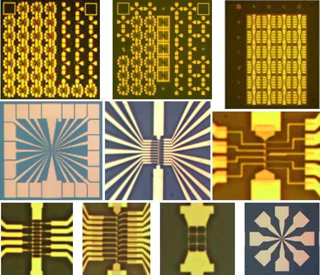
CHIP GALLERY: SEVERAL TYPES/KINDS OF CHIPS FABRICATED IN THE LAB
我々の研究室では、走査型プローブ顕微鏡(Scanning Probe Microscope: SPM)や電子線露光(Electron-Beam Lithography: EBL)を中心に、ナノメートル級の超微細加工技術を開発・駆使しながら、ナノテクノロジーやナノエレクトロニクスに関する研究活動を展開しています。 具体的には、原子を制御するナノテクノロジーを用いて、原子や電子を1個ずつ操作することが可能なナノエレクトロニクスシステムの研究や、機械学習や人工知能などの知能情報処理技術の支援による量子系(単電子帯電構造、トンネル接合、原子接合)での量子状態の制御に関する研究を行っています。 これらの技術をもとに、最近では、ナノギャップを用いて脳のシナプスを模倣したニューロモルフィックデバイスの開発や、量子計算機における量子・古典ハイブリッドアルゴリズムなどの変分量子アルゴリズムの開発とそれらを用いた組合せ最適化手法による量子実験系での実験パラメータ探索と原子接合の作製、量子計算機(量子アニーリングマシン)を模擬したFPGA実装型イジング計算機の実現と応用について検討しています。 以下に、代表的な研究内容のキーワードと簡単な解説を示します。また、実際の研究発表に関するタイトル詳細は研究業績やトピックなどをご覧ください。
OUR GROUP'S RESEARCH focuses on fabrication of nanodevices and measurement of their electronic and magnetic properties at low to room temperatures and includes new nanofabrication techniques, magnetoresistance properties in ferromagnetic nanodevices and transport properties of electrons through Si and metallic/ferromagnetic nanostructures such as quantum dots, atomic junctions and nanoconstrictions. Furthermore, new computing architectures using Ising spin model implemented on FPGA are also investigated. Monitoring human physiological signals using artificial flexible graphite thin films are recent research topics in our group.
KEYWORDS/RESEARCH TOPICS
Nanofabrication: Scanning Probe Microscopy (SPM), Atomic Force Microscopy (AFM), SPM Local Oxidation Nanolithography, SPM Scratching Nanolithography, Electron-Beam Lithography
Nanodevices: Single-Electron Transistor (SET), Ultra-Small Tunnel Junction, Quantum Point Contact (QPC), Ferromagnetic Nanostructure, Atomic Junction, Artificial Flexible Graphite Thin Film, Strain Sensor Based on Thin Graphite
Interesting Physical Properties: Single-Electron Charging Effects, Electromigration (Voltage-Controlled, Field-Emission-Induced), Magnetoresistance (MR), Anisotropic Magnetoresistance (AMR), Tunnel Magnetoresistance (TMR), Domain Wall Magnetoresistance (DWMR), Spin Injection/Current Induced Magnetization Reversal, Human Physiological Signal, Human Motion Detection, Vital Signs Sensing, Ising Spin Model, New Computing Architecture, Combinatorial Optimization Problem, Simulated Annealing, Quantum Annealing, Ising Computing, Quantum Computing/Computers, Variational Quantum Algorithm (VQA)
PhD DISSERTATION IN THE LAB
February, 2019
M. Ito "STUDY ON INTEGRATION OF ROOM-TEMPERATURE OPERATIONAL SINGLE-ELECTRON TRANSISTORS BY ELECTROMIGRATION IN SERIES-CONNECTED NANOGAPS"
February, 2018
M. Yagi "STUDY ON IN SITU MEASUREMENTS OF ELECTROMIGRATED METALLIC NANOCONTACTS USING ATOMIC FORCE MICROSCOPY"
August, 2017
R. Suda "STUDY ON REDUCTIVE DEPOSITION OF THIN FILMS BASED ON BALLISTIC ELECTRON INCIDENCE"
February, 2011
S. Nishimura "STUDY ON ADVANCED LITHOGRAPHY TECHNIQUES USING SCANNING PROBE MICROSCOPY FOR FABRICATION OF NANOSCALE Si DEVICES"
February, 2010
Y. Tomoda "STUDY ON PLANAR-TYPE FERROMAGNETIC NANOSCALE DEVICES FABRICATED BY NOVEL NANOFABRICATION TECHNIQUES"