
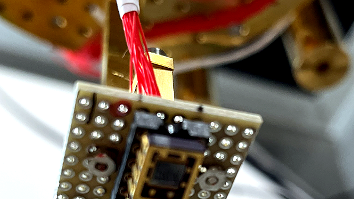
TUAT Takase Lab Quantum Physics and Engineering

Research Vision

高瀬研究室では、量子物性の解明と新しい学理の構築、量子状態を制御・計測する技術の開発を、相補的な研究の循環として捉えています。現象の理解が新しいデバイス・計測原理を導き、新しい技術が未知の量子現象を可視化します。この往復を通じて、量子科学と量子技術の新しい可能性を切り拓きます。

Takase Laboratory views the elucidation of quantum phenomena and the establishment of new physical principles, together with the development of technologies for controlling and measuring quantum states, as a complementary cycle. Deeper understanding leads to new device and measurement principles, while new technologies make previously inaccessible quantum phenomena observable. Through this interplay, we seek to open new possibilities in quantum science and technology.

Research themes

本研究室では、半導体ナノ構造、グラフェン、ダイヤモンド窒素空孔(NV)中心などの低次元・ナノ構造量子系を対象に、電子の電荷・スピン・軌道自由度:スピン軌道相互作用が生み出す量子輸送現象と、その制御・計測技術を研究しています。表面弾性波やラム波などの弾性波、マイクロ波やミリ波帯の高周波技術、NV中心の光検出磁気共鳴や電子スピン共鳴測定などを組み合わせ、量子自由度を「制御する」「測る」ことを通じて、新しい物性機能と量子デバイス原理の理解を目指します。

また、国内外の研究機関と連携し、材料・デバイス作製、量子輸送測定、スピン計測、理論解析を横断する共同研究を進めています。

Takase Laboratory studies low-dimensional and nanoscale quantum systems, including semiconductor nanostructures, graphene, and nitrogen-vacancy (NV) centers in diamond. Our research focuses on quantum transport phenomena arising from charge, spin, and orbital degrees of freedom, especially spin-orbit interaction, and on techniques for controlling and measuring these phenomena. By combining elastic waves such as surface acoustic waves and Lamb waves, microwave and millimeter-wave technologies, optically detected magnetic resonance of NV centers, and electron spin resonance measurements, we aim to understand new physical functions and quantum device principles through the control and measurement of quantum degrees of freedom.

We also pursue collaborative research with domestic and international institutions across materials and device fabrication, quantum transport measurements, spin measurements, and theoretical analysis.

Nanoscale semiconductor device

Quantum devices
Spin-orbit nanoelectronics

半導体ナノ構造では、電子の運動、スピン、電場が強く結びつくことで、バルク材料とは異なる量子輸送現象が現れます。本研究室では、ナノワイヤや微細加工デバイスを用いて、スピン軌道相互作用を電気的に制御し、スピン自由度を利用した新しいデバイス原理の理解を目指しています。電気伝導測定や低温測定を通じて、ナノスケールで電子がどのように動き、スピンがどのように制御されるかを調べます。 In semiconductor nanostructures, electron motion, spin, and electric fields are strongly coupled, giving rise to quantum transport phenomena that differ from those in bulk materials. We use nanowires and microfabricated devices to electrically control spin-orbit interaction and to understand new device principles based on spin degrees of freedom. Through electrical transport and low-temperature measurements, we study how electrons move and how spin can be controlled at the nanoscale.

Focused surface acoustic wave device simulation

Acoustic strain engineering
Structural strain engineering

グラフェンをはじめとする低次元材料を対象に、ひずみによる電子輸送特性の制御と量子デバイス機能の開拓を目指しています。特に、表面弾性波やラム波、機械振動子が生み出す動的ひずみに着目し、電子輸送やスピン・フォノン結合を制御する方法を研究します。これらの研究を通じて、低次元物質の基礎物性を理解するとともに、ひずみを利用した新しい量子デバイス原理の創出を目指します。また、動的ひずみに加えて、構造ひずみを用いたIII-V族半導体およびIV族半導体の物性制御にも取り組んでいます。 We study low-dimensional materials such as graphene and explore how strain can control electronic transport properties and enable quantum device functions. In particular, we focus on dynamic strain generated by surface acoustic waves, Lamb waves, and mechanical resonators, and investigate methods for controlling electronic transport and spin-phonon coupling. Through these studies, we aim to understand the fundamental properties of low-dimensional materials and to develop new quantum device principles based on strain. In addition to dynamic strain, we also study the control of material properties in III-V and group-IV semiconductors using structural strain.

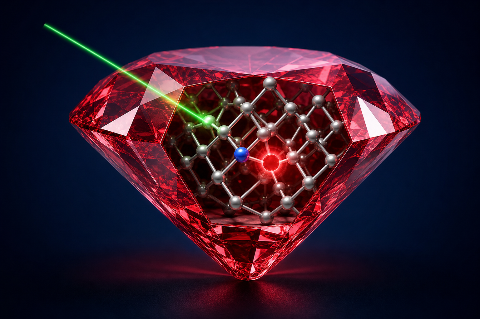
NV center schematic

Spin sensing
Quantum sensing and masers

ダイヤモンド中のNV中心は、電子スピンを光とマイクロ波で読み出せる量子センサーとして注目されています。本研究室では、NV中心を用いた光検出磁気共鳴測定を通じて、磁場・高周波場・スピン状態の計測技術を研究しています。低温・高磁場環境における高周波測定技術を新たに開発し、量子デバイスを「制御する」だけでなく、「測る」技術を発展させることを目指します。 NV centers in diamond are attracting attention as quantum sensors whose electron spins can be read out using light and microwaves. We study techniques for measuring magnetic fields, high-frequency fields, and spin states through optically detected magnetic resonance using NV centers. By developing high-frequency measurement techniques for low-temperature and high-magnetic-field environments, we aim to advance not only the control of quantum devices but also the technologies used to measure them.