
Abstract
The basic building blocks for brain-inspired computing are neurons and their inter-cellular connections, called synapses. In this paper, we report artificial synapses composed of simple gold (Au) nanogaps that function using an electromigration-based method called "activation." In the activation technique, metal-atom transport is induced by a field emission current, resulting in a change in gap separation. Synaptic functionalities, including long-term potentiation, long-term depression, and spike-timing-dependent plasticity, were successfully implemented in the electromigrated Au nanogaps using activation. Furthermore, the integration of four artificial synapses in a 2 × 2 array and image memorization were achieved with the Au nanogap-based artificial synapses. These results illustrate that electromigrated Au nanogaps hold promise as synaptic devices for bio-inspired computational systems.
Export citation and abstract BibTeX RIS
1. Introduction
The human brain can remember various details of past events, learn through stimulation from the external world, and process multidimensional information by a computational process with low power consumption and high error tolerance. Therefore, the idea of building an electronic system that can emulate the functions of the human brain has drawn significant attention in recent years.1–4) Generally, the essential functions of the human brain are performed by neurons and synapses.5–7) Synapses are the basic physical connections between different neurons, and thus, play a vital role in signal transmission. One fundamental property of a synapse is synaptic plasticity, which is the analog change in its efficacy when subjected to different input conditions. Therefore, the emulation of synaptic functions in a single electronic device is considered a key step toward realizing brain-like information storage and computing.8,9) In the last few years, there have been tremendous efforts to implement synaptic functions in various devices with memristive characteristics,10) such as magnetic tunnel junctions,11,12) phase-change devices,13,14) carbon nanotubes,15,16) memristors,17,18) and atomic switches.19,20) In addition to these electronic synapses, other candidates and new principles for artificial synapses have become appropriate for research. Importantly, the human brain contains as many as 1010 neurons. On average, each neuron is connected to 104 others through synapses,21) making the implementation of hardware with massively parallel electronic systems exceptionally challenging. In addition, artificial synapses should exhibit important synaptic learning rules, such as spike-timing-dependent plasticity (STDP), which is an essential feature of event-driven learning in brain-inspired computational systems.22)
In a previous study, we developed a simple technique for the fabrication of nanogaps with well-controlled tunnel resistance called "activation."23–30) This method is based on electromigration (EM) induced by a Fowler–Nordheim (F–N) field emission current. The activation scheme controls the tunnel resistance of the nanogaps by adjusting the magnitude of the field emission current. By utilizing the activation procedure with voltage pulses, the tunnel resistance of the nanogaps is expected to be incrementally modified, which resembles the learning procedure of biological synapses. From a physical point-of-view, the analog weight states in gold (Au) nanogaps using the activation method are enabled by the movement of metal atoms induced by the field emission current. Previously, we showed that synaptic devices of Au nanogaps that function using activation can be obtained, which allows for the implementation of several synaptic behaviors—notably, short-term plasticity and long-term plasticity.31) To enable the practical use of artificial synapses of Au nanogaps, implementation of a STDP learning rule and integration of Au nanogap-based synapses are required. In this study, we applied the activation procedure to Au nanogaps and demonstrated the experimental implementation of the basic synaptic functions of long-term potentiation/depression (LTP/LTD) and the STDP learning rule in simple Au nanogaps. Furthermore, the dynamic process of image memorization was mimicked through a 2 × 2 array of these synaptic Au nanogap devices.
2. Experimental methods
The initial single Au nanogaps and 2 × 2 nanogap arrays were fabricated on Si wafers coated with thermal oxide (thickness = 2 μm). First, the resist patterns were formed onto the surface of SiO2 using electron-beam lithography. Then, electron beam evaporation was used to deposit a Ti adhesion layer (5 nm), followed by the deposition of a 35 nm Au layer using a developed resist pattern as a template. Finally, the lift-off process was carried out to remove unnecessary metal and resist from the substrate. The gap separation of the fabricated Au nanogaps ranged from 40 to 130 nm. Before performing the activation, the Au nanogaps in the sample exhibited high tunnel resistances above 100 TΩ, which reflects the initial gap separation of the device.
After these fabrication processes, we performed the activation procedure and investigated the synaptic learning behaviors. The activation process was performed by applying a sequence of two different voltage waveforms: a voltage ramp for initializing the device resistances and voltage pulses for emulating synaptic functions.31) The sequence of steps for the activation process with a voltage ramp has been described in detail in our previous papers.23–25) After performing the activation procedure with the voltage ramp, trains of identical voltage pulses were applied to the Au nanogaps, and the conductance was continuously monitored by a reading operation after each pulse. Electrical characterizations of the Au nanogaps were carried out at room temperature using a semiconductor parameter analyzer (Keysight B1500A). Scanning electron microscopy (SEM) images were taken on a HITACHI S-4500 field-emission SEM at an accelerating voltage of 20 kV.
3. Results and discussion
A conceptual schematic diagram of a biological synapse and inorganic synapse using electromigrated Au nanogaps is illustrated in Fig. 1. Here, there is an intriguing analogy between the motion of the vesicles in the synaptic junctions and the migration of Au atoms occurring upon resistance switching. When an action potential of the pre-synaptic neuron reaches the synapse, a neurotransmitter is released into the synaptic cleft, which binds to neurotransmitter receptors on the post-synaptic neuron side and precisely changes the connection strength between the neurons.32) In the simplest Au nanogaps, the source and drain electrodes work as the pre- and post-synaptic neurons, respectively. By applying a voltage to the nanogap electrodes, an F–N field emission current is induced in the Au nanogap. Then, the Au atoms at the tip of the source electrode are activated by the field emission current, resulting in the accumulation of atoms within the gap. The separation of the nanogap electrodes after performing activation becomes smaller than that beforehand. As a result, the tunnel resistance of the nanogap decreases. Hence, the Au nanogaps controlled by activation are expected to have adaptive resistance, which would enable the device to mimic biological synaptic plasticity.

Fig. 1. (Color online) Schematic illustration of Au nanogaps with the activation method as synapses from a structural analogy point-of-view. A biological neuron transmits information via propagation of action potentials through the axon and release of neurotransmitters at nerve synapses. The synaptic connection is incrementally modulated via neurotransmitter migration through the synapse cleft. In the case of Au nanogaps, the migration of Au atoms from the source to the drain electrode is induced by a Fowler–Nordheim field emission current. The conductance of the Au nanogaps gradually changes via the migration of activated Au atoms.
Download figure:
Standard image High-resolution imageThe conductance of the Au nanogaps gradually changes under the application of stimulation pulses. As shown in Fig. 2(a), we applied four positive voltage pulses with an amplitude V = 58 V, duration W = 25 ms, and period t = 3 s to examine the synaptic weight response of the Au nanogaps. Upon the application of each voltage pulse stimulation, the device conductance increases abruptly at the beginning, rapidly decays to a lower level, and finally stabilizes to an intermediate state. However, the overall current increases with the application of positive voltage pulses; this conductance change is similar to that of the memory enhancement in biological synapses. This result corresponds to our previous observations, as reported in Ref. 31. In contrast, as shown in Fig. 2(b), current response spikes and rapid decay occur when negative voltage pulses with an amplitude V = −54 V, duration W = 25 ms, and period t = 3 s are applied to the Au nanogaps. In accordance with this decay process, an overall depression in the device conductance with the number of negative voltage stimulations occurred. These results indicate that the connection weight of the Au nanogaps becomes potentiated or depressed with consecutive positive or negative stimuli, respectively.

Fig. 2. (Color online) Au nanogap response to programming pulses. Current response as a function of time recorded under (a) positive and (b) negative voltage pulse stimulations exhibiting the spike response, spontaneous decay, and overall potentiation or depression in device conductance. The conductance of the device after each pulse was recorded at 29 V to avoid significant disturbance to the device state.
Download figure:
Standard image High-resolution imageThe gradual changes in the conductance of the Au nanogaps was further studied. Figure 3 shows the current variation induced by applying trains of identical positive stimulation pulses (58 V, 25 ms), followed by a series of identical negative stimulation pulses (−46 V, 25 ms). A shorter interval time (t = 0.25 s) between programming pulses was used during potentiation for long-lived transition to the higher-conductance state,31) while a longer interval (t = 3 s) was used during depression to utilize the decay behavior of the nanogap current. The change in device current was detected at 34 V just before the next programming pulse. Therefore, the interval times between the read pulse and the programming pulse are 130 ms and 2.9 s for positive and negative pulses, respectively. As expected from the results in Figs. 2(a) and 2(b), the application of positive stimulation pulses incrementally increases the device current, and the application of negative stimulation pulses gradually decreases the device conductance. This incremental tuning of the device current denotes an alteration in synaptic weight in response to positive or negative voltage pulses. Such enhancement and diminishment characteristics are consistent with the LTP and LTD observed in biological synapses, respectively. The gradual changes in the conductance of this artificial synapse may occur because of the migration of Au atoms induced by the engineered input voltage pulses. However, there is still some room of discussion on the model of the phenomena and possible other mechanisms should be considered.33–37)

Fig. 3. (Color online) Device current in response to a series of potentiating and depressing voltage pulse stimulations, showing the respective enhancement and weakening of the synaptic strength. All current data were measured using a small read voltage amplitude of 34 V after each pulse excitation. The first data point is the initial unexcited current level.
Download figure:
Standard image High-resolution imageAfter characterizing the basic memristive properties of the Au nanogaps using the activation technique, we proceed to demonstrate the activity-dependent plasticity of our electronic synapse. Synaptic plasticity, which is believed to account for learning and memory in the biological brain, refers to the change in connection weight (ΔW) over time in response to action potentials. One of the most important timing-based functions of the nerve synapse is the STDP learning rule, which is based on Hebbian learning.38) STDP is a modulation of the synaptic weight in response to the relative timing between pre- and post-spikes, Δt. Persistent augmentation of synaptic strength (LTP) occurs if a pre-neuron spikes before a post-neuron (i.e., Δt > 0), whereas a decrease in synaptic strength (LTD) occurs when a post-neuron spikes before a pre-neuron (i.e., Δt < 0). In addition, both the potentiation and depression of the synaptic connection weights exhibit negative dependence on the spike timing difference, where a smaller timing difference leads to a larger increase (or decrease) in synaptic weight.
Figure 4(a) shows the shape of the pre- and post-spikes used for the implementation of STDP learning. The superimposition between the pre-spike and the post-spike (Vpost–Vpre) defines the total effective voltage applied to the Au nanogap. When pre-synaptic firing precedes the post-synaptic spike, a large positive pulse is applied, whereas a negative pulse is applied when the post-synaptic spike precedes the pre-synaptic spike. Figure 4(b) exhibits the measured relative changes in the synaptic weight (ΔW) of the Au nanogaps, defined as the ratio of the difference between the current values before and after injecting the stimulation spikes. It can be inferred that the STDP learning rule was successfully reproduced in our electronic synapse by applying the stimulation voltage spikes. The largest synaptic weight changes occurred when the relative timing of the spike arrival (Δt) was small. Consequently, Au nanogaps using activation store the timing information as a relative change in conductance, which represents the long-term nonvolatile memory of synaptic functionality. Generally, the STDP time window in biological synapses has been described by the following equation:39)

where ΔW is the percentage change in synaptic weight; Δt is the pre-/post-spike time difference; and  and
and  are the scaling factor and time constant, respectively. The solid line in Fig. 4(b) is the fitted exponential curve. The experimental data are well expressed using Eq. (1) with
  and
and  ms. It is expected that, by designing the pulse schemes, the time constant of the STDP window could be modulated across a wide temporal range.13) Therefore, electronic synapses of Au nanogaps could be suitable for designing complex cognitive systems and neuromorphic circuits.
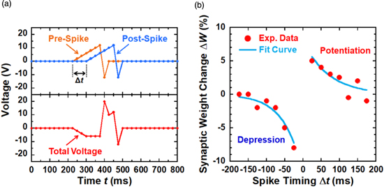
Fig. 4. (Color online) STDP implementation. (a) Stimulation spike schemes used to implement STDP. The upper plot shows a part of the pre- and post-spikes with a 75-ms positive temporal difference. The lower plot exhibits the net programming voltage applied to the Au nanogaps. (b) Weight modulation of Au nanogaps as a function of the relative timing between pre- and post-synaptic spikes. Symbols: experimental results obtained from the average of 50 stimulations. Solid lines: exponential fits of the experimental data.
Download figure:
Standard image High-resolution imageFigure 5(a) shows a SEM image of an initial Au nanogap electrode before performing the STDP learning operation. Compared with the SEM image of an Au nanogap after the STDP learning operation using activation, the gap separation narrows from approximately 46 nm to less than 10 nm, as shown in Fig. 5(b). Furthermore, after performing the activation procedure, a difference in contrast was observed between the tips of the source and drain electrodes. During the initialization process and application of positive pulses, the field emission current moves the activated Au atoms from the source to the drain electrode. Consequently, activated Au atoms accumulate at the tip of the drain electrode, resulting in LTP. In contrast, in the case of negative pulses, activated Au atoms migrate from the drain to the source electrode, which is the opposite behavior to that demonstrated in the positive pulse case. Therefore, it is expected that the application of negative pulses will drive accumulated Au atoms away from the tip of the drain electrode, thereby decreasing the synaptic weight. This could be the main mechanism of the LTD behavior observed in the Au nanogaps. However, further study will be necessary to elucidate the mechanisms of LTP and LTD mimicked by the Au nanogaps using the activation method.

Fig. 5. SEM images of typical Au nanogap electrodes (a) before and (b) after activation and STDP learning process for mimicking the synaptic plasticity. The STDP learning includes the potentiation and depression processes. Upon applying positive pulses, Au atoms at the tip of the source electrode migrate from the source to the drain electrode across the gap. Upon applying negative pulses, the field emission current move the Au atoms from the drain to the source electrode.
Download figure:
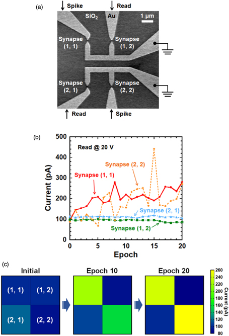
Standard image High-resolution imageBased on the learning behaviors of the Au nanogaps using activation, the dynamic process of memorizing pixel images was mimicked through a fabricated passive 2 × 2 array of Au nanogaps [Fig. 6(a)] in order to demonstrate the trainable memory behaviors. Figure 6(b) shows the changes in the current of the synapses during the learning procedure. The image pattern was stored using positive voltage pulses with an amplitude of 57 V for synapse (1, 1) and 55 V for synapse (2, 2), duration W = 25 ms, and period t = 0.25 s. The amplitudes of the training pulses used for input stimulations were optimized for individual synapses. A low read voltage of 20 V was applied to synapses (1, 2) and (2, 1) during the learning process. As shown in Fig. 6(b), pattern weights [synapse (1, 1) and synapse (2, 2)] tend to adopt a high conductance state through repeated stimulations, whereas background weights [synapse (1, 2) and synapse (2, 1)] remain in a low conductance state and are unaffected. Here, the fluctuation of the change in the current can be seen in synapse (2, 2). Furthermore, a device-to-device variation of the learning behavior appeared: synapse (1, 1) did not show such severe fluctuations. This fluctuation may be caused by a series of structural relaxations as the Au atoms at the very end of the electrodes switch from one stable configuration to another40) upon migration and accumulation of Au atoms. Figure 6(c) exhibits the progression of the synaptic weight map during the memorization process. Herein, the memorized information is represented by the current level of the Au nanogaps. To begin, the four synapses of Au nanogaps were initialized to small weights and exhibited a relatively uniform initial current level of approximately 100 pA by applying a read voltage of 20 V, as shown in Fig. 6(c). Then, a checkerboard pattern was programmed into the array of Au nanogaps to memorize the image. As illustrated in Fig. 6(c), after the 10th training process, the current of the artificial synapse begins to diverge, and the conductance of the stimulated synapse is slightly enhanced. Therefore, the input image begins to emerge on the readout current map. After the 20th training epoch, the current level of the stimulated synapse is further increased, indicating a deeper memory of the checkerboard pattern. The final current level of the selected synapse tends toward stability, and the input checkerboard pattern is strongly memorized. Furthermore, the strengths of the potentiated synapses last for at least 2 s. Therefore, it is suggested that synaptic device arrays of Au nanogaps can be used to implement relatively complex functions of the brain, for example, image memorization and associative memory.
Fig. 6. (Color online) Image memorization into an artificial synapse array. (a) SEM top-view image of the fabricated circuit. (b) Measured synaptic weights as a function of the number of training epochs. (c) Changes in cell currents during the memorization procedure. All synapses were initialized to a high-resistance state with some stochastic variation before the learning process. An image of a checkerboard pattern was memorized simultaneously into a 2 × 2 synapse array by inputting the image 20 times using positive stimulation pulses with an interval of 0.25 s.
Download figure:
Standard image High-resolution image
4. Conclusions
In conclusion, we implemented synaptic plasticity in simple Au nanogaps that enable continuous changes in the device conductance using a unique technique based on EM induced by a field emission current. Our artificial synapse of Au nanogaps behaves as a nerve synapse and exhibits the characteristics of LTP, LTD, and the STDP learning rule. The complex learning capability of the Au nanogap-based artificial synapses was demonstrated through pattern memorization with a 2 × 2 array. These synaptic behaviors are achieved with high electrical performances, such as a relatively low programming current (∼nA). As mentioned above, the important synaptic functions achieved in the present device satisfy the basic requirements for brain-inspired computing architecture. However, more efforts should be devoted in the future to the design and construction of interconnected networks of artificial synapses of Au nanogaps for large-scale neuromorphic circuits. Above all, owing to its simple structure, we believe that the demonstrated synaptic device of Au nanogaps using activation will open the possibility of realizing novel neuromorphic learning systems based on nonlinear spike-based processing that can mimic biological processes.